Manufacturing Developments at Display Week 2007 Focus on Improving Economics and Expanding Capabilities
from the Information Display Manufacturing section
Yield and capacity are two of the key metrics discussed in the area of display manufacturing. But how are advances in these two areas achieved? That was the focus of myriad presentations and exhibits at Display Week 2007, where lowering costs and expanding capabilities for display manufacturing took center stage.
This past May’s Display Week 2007 produced many exciting announcements, demos, and papers that focused on advances in the manufacture of displays. The manufacturing advances appeared along two axes. The first axis focused on improving the economics of the manufacturer, i.e. the utilization of a specific equipment, process, or materials that would result in a productivity improvement, capital avoidance, or a lower cost of ownership at the display manufacturer’s site. The second axis concentrated on delivering enabling capability or a tool/technique that would afford the owner the ability to make a display or display component that previously was accomplished with difficulty, or not at all.
Improvement of Display-Manufacturer Economics
The vendors that focused on improved economics largely did so via developments in equipment and process. These companies included Nakan, New Way Air Bearings, Powerlase, and KLA Tencor.
Nakan promoted its recently released tool sets for Gen 6 and 7 glass and described its latest design (six patents pending) for alignment layer tools. In this design, the alignment layer deposition is achieved with a moving-plate cylinder in the printing operation. Nakan has achieved a performance of 40 sec per sheet in both its Gen 6 and 7 tools.
New Way Air Bearings showed three modular air bearing products designed to meet non-contact glass-handling requirements for manufacturing. The differentiated technical approach relies on porous carbon. The porous-carroach controls the airflow across the entire bearing surface through millions of holes in the porous material. New Way Air Bearings has found porous carbon to be one of the best materials for this purpose, producing an ideal supply of uniform air pressure across the face of the bearing while automatically restricting and damping the air flow at the same time. The carbon surface (Fig. 1) provides greater bearing protection in the event of an air-supply failure and allows the bearings to be moved during air failure without damaging the support surface.
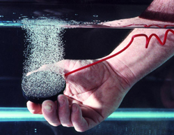
These conveyor air bearings have been employed for a variety of tasks in flat-panel-display manufacturing, including floating glass at high speeds, incorporation into low-air-flow conditions, and precision processes such as alignment. The non-contact handling method improves yield and product reliability compared with contact methods of handling (Fig. 2).
KLA Tencor described its P16+ surface-profiler tool, which is used to test the integrity of thin-film and chemical-coating surefaces. KLA Tencor’s tool is vital for capturing a display manufacturer’s yield-critical defect and metrology data. Recently released software speeds the analysis. The latest device configuration permits samples 19 inches in length to be analyzed.
Powerlase, Ltd., claimed its rapid laser patterning (RLP) of ITO on glass for plasma-display manufacturing provides a cost-effective alternative to wet-etch lithography. Powerlase outlined the incumbent wet process and the proposed alternative (Fig. 3 – Not Included).
Clearly, there are fewer steps in the laser process, and this typically bodes well for cost savings. Powerlase went on to describe improvements in the plasma-display manufacturer’s cost of ownership largely achieved via yield improvements. These yield improvements more than offset the cost of the laser system.
When applied to liquid-crystal-display (LCD) manufacturing technology, AU Optronics Corp. (AUO) employed a laser process in conjunction with ITO patterning. AUO incorporated an excimer laser into the back-channel-etch amorphous-silicon thin-film-transistor (a-Si TFT) fabrication. Similar to the Powerlase approach, AUO proposes this process as a potential replacement for the traditional chemical processing for ITO patterning and points out the potential benefits in the reduction of masks.
New Updated Manufacturing Capabilities
Companies including Nanogram, Dupont, Samsung SDI, and Dai Nippon Screen provided Display Week 2007 attendees with updates on manufacturing, process, and material technologies that bring new capabilities to a variety of techniques and devices. In addition, several technical papers focused on laser transfer as well as ink-jet technologies.
Nanogram described a series of silicon inks for a variety of products. The chemical sets included doped nanoparticle silicon and next-generation liquid silicon. Nanogram is focused on delivery systems including ink-jet, spin-on, and roll-to-roll capability. The product roadmap calls for these inks to start with passive components with the display-market targets of TFTs for electronic paper and electronic books. Ultimately, Nanogram is targeting transistors for polymer organic-light-emitting-diode displays (PLEDs) – a critical component for a fully printed active-matrix display.
Dupont presented a new maskless, completely dry color-filter manufacturing system for LCDs based on breakthrough direct laser-writing technology. Dupont leverages its thermal-imaging transfer mechanism to achieve the dry process, which eliminates liquid handling and photomasks, reduces process steps, and minimizes the clean-room footprint. This new technology significantly reduces process steps and clean-room space required by conventional photolithography, thereby providing significant capital and operational savings. Since the system is based on digital technology, the direct-writing precision-patterning process eliminates photomasks for RGB, is highly scalable, and greatly simplifies pattern changeover.
Samsung SDI explained its progress of developing a laser-induced thermal imaging (LITI) process for the manufacturer of active-matrix OLEDs (AMOLEDs). The application of the LITI process for OLED manufacture included the development and optimization of transfer films, the resulting OLED layers, as well as the scanning conditions for the patterning of the evaporated small molecules. samsung SDI achieved improved device characteristics attributable to the employment of the LITI process. Further, Samsung SDI took this manufacturing development further by setting up a Gen-4-sized LITI system (Fig. 4 – Not Included).
Sony showed off a 27.3-in. AMOLED fabricated using a process called laser-induced pattern-wise sublimation (LIPS). In this process, OLED materials are transferred from glass donors to a substrate by the process. As with the previously mentioned laser techniques, the pixels are precisely patterned. Sony achieved impressive results with respect to the device performance. The atmospheric conditions associated with the sublimation process appear, however, to need some slight improvement to achieve the desired overall reliability (Table 1 – Not Included).
Spacer manufacturing has historically been a perplexing problem for would-be field-emission-display (FED) manufacturers and a relevant area of interest for plasma-display-panel (PDP) manufacturers. During the Display Week 2007 Symposium, Dai Nippon Screen described a new nozzle-dispense method for fabricating spacers. Spacers are characterized as high-aspect-ratio insulators used to maintain the vacuum gap and separate the anode and cathode in an FED. Typically, spacers are the result of machining, cutting, and dicing of ceramic or glass materials. Dai Nippon Screen showed a nozzle-based method of dispensing a slurry, baking, and curing to achieve the requisite structure (Fig. 5 – Not Included).
Ink-jet manufacturing techniques were highlighted for a variety of advanced processes, components, and devices. The technical advances for printed transistors are characterized not only by new materials but also by their delivery via ink-jet printing. In general, ink-jet-technology is being used to achieve a wider variety of device architecture as well as component functionality. With wider use, the fundamental ink-jet technology is being improved. Litrex in conjunction with Cambridge Display Technologies (CDT) described improvements in drop-landing accuracy achieved via improved equipment design. Surely, these improvements will positively impact the variety of applications and components that are currently exploring ink jet as a means of manufacturing.
Summary
From a display manufacturing point of view, Display Week 2007 provided an overview of industry developments designed to improve the economics of manufacturing. In addition, many of the manufacturing advances described will ultimately impact the performance that display consumers will benefit from. The exhibits as well as the presented materials highlighted the relentless drive of the display industry’s movement of R&D ideas through process and manufacturing developments.
Peter Smith is with Honeywell, Inc. 101 Columbia Road, CTC 3-003, Morristown, NJ 07962; telephone 201.454.1786; email: peter.smith@honeywell.com
by Peter Smith
Honeywell, Inc. 101 Columbia Road, CTC 3-003, Morristown, NJ 07962